What does microlithography mean?
What does microlithography mean? A spoken definition of microlithography. Intro Sound: Typewriter - Tamskp Licensed under CC:BA 3.0 Outro Music: Groove ...
What Does That Mean?
High purity microlithography chemicals
As the semiconductor and flat panel display industry moving to finger geometry, the demand of electronic chemicals has been expended.
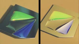
Etching Gold
How are tiny computer chips made? Nanolithography explained
Want to learn more about nanoscience and nano technologies? Visit Curiosity Machine for lesson plans, engineering activities, and more: ...
Technovation
How To Say Microlithography
Pronunciation of Microlithography: Learn how to pronounce the word Microlithography. Definition and meaning can be found here: ...
Emma Saying
Video 27: Soft Lithography Case Study
Note: Watching in HD 1080 and full screen is strongly recommended. *** MIT RES.10-001 Making Science and Engineering Pictures: A Practical Guide to ...
MIT OpenCourseWare
Electron Beam Lithography
How does E-beam lithography work? What are the differences compared to photolithography?
Raith GmbH
Towards Integrated Optical Time Standards and Frequency Synthesizers, by Kerry Vahala
By: Kerry Vahala (Ted and Ginger Jenkins Professor of Information Science and Technology and Professor of Applied Physics, CalTech) Abstract: ...
IEEE-UFFC
Optics Tutorial - 2 - Lens and focusing basics
Introduction to focusing light: 1) Spherical surface refraction 2) Anatomy of a lens (and a mirror) 3) Focal length 4) Sign of the focal length 5) Computing a "thin ...
opticsrealm
How to Pronounce Microlithography
This video shows you how to pronounce Microlithography.
Pronunciation Guide
Kafai Lai: Exploring technology solutions with computational lithography
Next-generation lithography requires more sophisticated design tools. http://spie.org/al - SPIE Advanced Lithography Symposium Kafai Lai is Senior Scientist ...
SPIETV
Colloquium: John Bruning - Phase Measuring Interferometry – Roles in the microelectronics...
Title: Phase Measuring Interferometry – Roles in the microelectronics revolution and astronomy Abstract(s): The microelectronics revolution has been ongoing ...
UA OSC
Will Tong: Alternative lithographic techniques
Advancing lithography to smaller and smaller dimensions will require a multidisciplinary approach and openness to new techniques. http://spie.org/al - SPIE ...
SPIETV
Intro to the Journal of Micro/Nanolithography, MEMS, and MOEMS from the Editor-in-Chief, Chris Mack
SPIE Journal of Micro/Nanolithography, MEMS, and MOEMS - http://spie.org/x865.xml The Journal of Micro/Nanolithography, MEMS, and MOEMS (JM3) ...
SPIETV
Nanofabrication Techniques: Electron Beam Lithography
NFFA-EUROPE for nanoeducation - lectures and training courses on the specialised technology and fine analysis techniques available through NFFA-EUROPE.
NFFA Europe
Dow Chemical - Dow AR™ Fast Etch Organic Bottom Antireflectant Coatings
In this video, The Dow Chemical Company's Timothy Adams, Suzanne Coley, Vipul Jain, Doris Kang, Amy Kwok, Owendi Ongayi, Edward Pavelchek, James ...
ACS Heroes of Chemistry
Hakaru Mizoguchi: Development of 250W EUV Light Source for HVM Lithography
A plenary talk from SPIE Photonics West 2017 - http://spie.org/PW In this plenary session, Hakaru Mizoguchi of Gigaphoton Inc. (Japan) discusses the ...
SPIETV
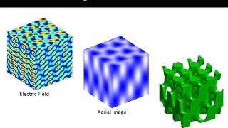
Lecture 17 (EM21) -- Holographic lithography
This lecture describes holographic lithography and how to design four beams whos interference pattern can be used to fabricate any of the 14 Bravais lattices.
CEM Lectures
The NLP2000 Dip Pen Nanolithography System from Nanoink
The NLP2000 Dip Pen Nanolithography system as shown at its launch at Pittcon 2009.
AZoTV
Lecture 38 (CHE 323) Lithography Introduction
Lithography: Introduction.
Chris Mack
Photolithography Overview for MEMS
This is a short overview of the photolithography processes used to fabricate micro-sized devices. This presentation was produced by the Southwest Center for ...
Support Center for Microsystems Education
Old World Labs FULL HD
Old World Labs Microlithography, Microfabrication, High-Resolution 3D Printing, Mass Scale Additive Manufacturing,
Old World Labs
NanoInk's 3D DPN Animation
This animation demonstrates how Dip Pen Nanolithography (DPN) works using NanoInk's lithography instruments. The benefits of DPN are highlighted along ...
nanoINKtv
Synopsys Optical and Photonics Solutions Groups, 57 Years of Innovation in the Simulation of Light
Speaker: Dr. Jake Jacobsen Abstract: Optical Research Associates started in 1963 with a crazy idea that you could, maybe, trace rays faster and better with ...
UA OSC
EML Webinars by Stephanie Lacour on soft neural interfaces
EML Webinar on July 8, 2020 was given by Prof. Stephanie Lacour at EPFL via Zoom meeting. Discussion leader: Sigurd Wagner, Princeton University Title: ...
EML Webinar
Tricks in Lithography : Part 1 (Immersion Lithography)
Resolution Enhancement Techniques : Part 1 Immersion Lithography.
nanolearning
Future Applications of DPN
Potential applications for DPN.
azonano
Enterprise Architecture l José Pires l at BTOES l a Proqis Company
ABOUT BTOES INSIGHTS *** BTOES Insights is a professional online content platform for Business transformation & operational excellence professionals.
BTOES Insights
Micromanufacturing Meaning
Video shows what micromanufacturing means. The manufacturing of components or devices on a micro scale, especially by the use of microlithography.
ADictionary
e-Beam Lithography
Alexandr Kolesnikov
Nanoimprint lithography (NIL) at DTU
Video shows activities from the course Nanolithography at DTU.
DTU Nanotech Optofluidics
The Process of Making Breakthroughs in Engineering by Thomas Kailath: The 1st Wook Hyun Kwon Lecture
2016.09.23.
ERC-ACI, Seoul National University
Doug Resnick: Acquisition opens new semiconductor capabilities
Molecular Imprints was acquired by Canon in April 2014, allowing Canon to participate in accelerated development of next-generation semiconductor ...
SPIETV
Bi-layer Lift-off Process - A-Gas EM
A-Gas EM Troubleshooter.
A-Gas Electronic Materials
Soft Lithography
This video is about IMG_0623.
Eric Pei-Yu Chiou
What is nanotechnology and nanoscience | explained in hindi | class X science and technology
Hello, Know what is nanotechnology and nanoscience in hindi. Know everything about nanotechnology. Class X science and technology. Mathematically 1 ...
KnowTalks
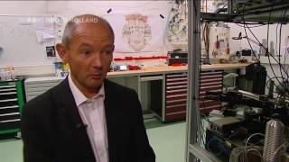
#OnsNoordHolland ECONOMIE - Nanolithografie
Weet jij wat nanolithografie is? Met een bijdrage aan het Advanced Research Center Nanolithograpy wil de provincie innovatie stimuleren en werkgelegenheid ...
Provincie Noord-Holland
SCIL Nanoimprint lithography
For more information visit www.miplaza.com.
SemiconEurope
How AFM Works 8-4 Nanolithograpy
Here, the cantilever is used to intentionally modify the sample surface via mechanical and/or electrical means. To mechanically alter a surface, a specialized, ...
Park Systems
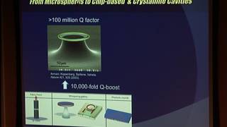
Colloquium: Kerry Vahala
"Confining Light on a Chip: The Science of Optical Microresonators" Abstract(s): Like a tuning fork for light, optical resonators have a characteristic set of ...
UA OSC
Advanced Force Microscopy and Nanolithography. ForceTool. ICMM-CSIC
The research activity of this group is focused on the development of analytical tools and methodologies based on scanning probe technology for exploring the ...
icmm csic
EP1: PiFM @ Work - Nanoscale Silicon Strain Measurements
Episode 1: Nanoscale Silicon Strain Measurements explores silicon oxide stress using the Vista-IR microscope. Photo-induced Force Microscopy - Series - PiFM ...
Molecular Vista
Measurement Challenges arising from New SemiconductorMaterials (...) | Dr. Alain Diebold | 2018NSSUS
Title: Measurement Challenges arising from New Semiconductor Materials and Structures for Integrated Circuits Speaker: Dr. Alain Diebold, SUNY Polytechnic ...
Park Systems