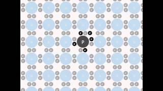
Tutorial: Doping
MIT 2.627 Fundamentals of Photovoltaics, Fall 2011 View the complete course: http://ocw.mit.edu/2-627F11 Instructor: Joe Sullivan Pure silicon has very low ...
MIT OpenCourseWare
What is Materials Engineering?
STEMerch Store: https://stemerch.com/Support the Channel: https://www.patreon.com/zachstar PayPal(one time donation): https://www.paypal.me/ZachStarYT ...
Zach Star
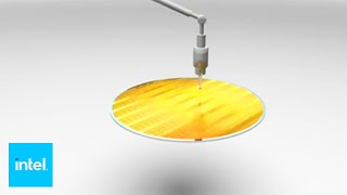
From Sand to Silicon: the Making of a Chip | Intel
This is how a microprocessor, the brain 'behind the magic' of your PC, is made. For more about process Intel employs in building the chips that power many of ...
Intel
Chip Manufacturing - How are Microchips made? | Infineon
How are microchips made - from sand to semiconductor: Microelectronics usually is hidden to society – however, it is a constant companion in our daily lives.
Infineon Technologies AG
From Sand to Silicon: The Making of a Microchip | Intel
Ever wonder what's under the hood of your favorite electronic device? The transistor is the engine that powers every Intel processor. To build a modern computer ...
Intel
Predictive Simulation of Semiconductor Processing Status and Challenges Springer Series in Materials
kemal nikon
Mod-02 Lec-06 Basics of Semiconductor and Process flowchart; Video on "Sand-to-Silicon"
An Introduction to Electronics Systems Packaging by Prof. G.V. Mahesh, Department of Electronic system Engineering, IISc Bangalore.For more details on ...
nptelhrd
Compound Semiconductor Epitaxy Research at Nokia Bell Labs
Go behind the scenes of the Nokia Bell Labs III-V Lab in France to learn about the compound semiconductor epitaxy research we are conducting.
Nokia Bell Labs
Professor Alberto Salleo: Materials Science at Stanford: The beginning of the next century
Stanford University School of Engineering
Mod-01 Lec-11 Compound Semiconductors
Processing of Semiconducting Materials by Dr. Pallab Banerji,Department of Metallurgy and Material Science,IIT Kharagpur.For more details on NPTEL visit ...
nptelhrd
Metals & Ceramics: Crash Course Engineering #19
Today we'll explore more about two of the three main types of materials that we use as engineers: metals and ceramics. We'll discuss properties of metals, alloys ...
CrashCourse
Developing New Semiconductor Materials as Magnets to Realize Semiconductor Spintronics
Keio Spintronics Network - Kuroda Laboratory , University of Tsukuba Graduate School of Pure and Applied Sciences (Materials Science and Engineering)] At ...
慶應義塾Keio University
Introduction to Materials Science for MEMS and NEMS - Part 1
Join Spaceport Odyssey iOS App for Part 2: https://itunes.apple.com/us/app/spaceport-odyssey/id1433648940 Join Spaceport Browser for Part 2: ...
SpaceChallenges
12. Thin Films: Material Choices & Manufacturing, Part I
MIT 2.627 Fundamentals of Photovoltaics, Fall 2011 View the complete course: http://ocw.mit.edu/2-627F11 Instructor: Tonio Buonassisi This lecture introduces ...
MIT OpenCourseWare
Lecture 1 (CHE 323) Semiconductor Overview
Semiconductor Overview.
Chris Mack
Department of Materials Science and Engineering, Seoul National University
SNU-MSE, Enabler of Economic Growth of South Korea. South Korea achieved great economic success in many aspects. It is the only country in the world who ...
WebsEdge Science
Intro to sputtering (process to create clear, conductive coatings)
I have finally been successful in creating a conductive, clear layer of indium-tin oxide on a microscope slide. In this video, I show the process and explain how ...
Applied Science
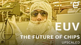
EUV: Lasers, plasma, and the sci-fi tech that will make chips faster | Upscaled
Microchips are one of the most complicated objects humanity has created, packing billions of transistors into a chip only a few centimeters across.
Engadget
Introduction to Department of Metallurgy, Materials Science, and Materials Processing (English ver.)
Introduction to Department of Metallurgy, Materials Science, and Materials Processing, School of Engineering, Tohoku University 東北大学工学部材料科学総合 ...
東北大学
The Polymer Explosion: Crash Course Engineering #20
We're continuing our look at engineering materials with third main type of material that you'll encounter as an engineer: polymers. They're made of long, ...
CrashCourse
Semiconductor introduction
How N-type and P-type semiconductors are made of silicon doped with phosphorous or boron.
Khan Academy
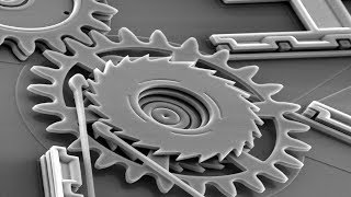
The Extreme Physics Pushing Moore’s Law to the Next Level
A look inside a new precision machine that wants to reinvent the chip making industry. »Subscribe to Seeker! http://bit.ly/subscribeseeker »Watch more Focal ...
Seeker
Lean Six Sigma In 8 Minutes | What Is Lean Six Sigma? | Lean Six Sigma Explained | Simplilearn
In this video, we'll tell you everything you you need to learn about Lean Six Sigma in 8 minutes! We'll be covering a number of major concepts like Lean and Six ...
Simplilearn
391 San Antonio Rd.—A Semiconductor Documentary
Silicon Valley is known worldwide as the global center of high tech innovation. In large part, the spark that ignited Silicon Valley's explosive growth can be traced ...
Computer History Museum
The Legacy of Fairchild Semiconductor
[Recorded Oct 5, 2007] Founded in September 1957 in Palo Alto, California by eight young engineers and scientists from Shockley Semiconductor Laboratories, ...
Computer History Museum
What Are Semiconductor Materials?
https://www.fiberoptics4sale.com Semiconductors are made up of individual atoms bonded together in a regular, periodic structure. The electrons surrounding ...
Fiber Optics For Sale Co.
Mod-01 Lec-01 Introduction
Advanced ceramics for strategic applications by Prof. H.S. Maiti,Department of Metallurgy and Material Science,IIT Kharagpur.For more details on NPTEL visit ...
nptelhrd
Master of Science in Applied Physics and Applied Mathematics
Learn about the fields of study available in Columbia Engineering's Applied Physics, Applied Mathematics, and Materials Science and Engineering master's ...
Columbia Engineering
How do SSDs Work? | How does your Smartphone store data? | Insanely Complex Nanoscopic Structures!
Have you ever wondered how your smartphone can store countless pictures, songs, or videos? Or, have you wondered when you download a podcast to your ...
Branch Education
Neuromorphic Computing Is a Big Deal for A.I., But What Is It?
Engineering computers to work like brains could revolutionize technology as we know it. Here's everything you need to know about neuromorphic computing.
Seeker
How Does Electroplating Work | Reactions | Chemistry | FuseSchool
How Does Electroplating Work | Reactions | Chemistry | FuseSchool Learn the basics about electroplating. The anode is positively charged, and the cathode is ...
FuseSchool - Global Education
Mod-03 Lec-21 Carrier recombination-generation-I: band-to-band transition
Optoelectronic Materials and Devices by Prof. Monica Katiyar & Prof. Deepak Gupta,Department of Metallurgy and Material Science,IIT Kanpur.For more details ...
nptelhrd
The Department of Applied Physics at Yale University - Excelling in Research and Mentoring
The Department of Applied Physics at Yale University is a great place to do graduate and postdoctoral study. Applied Physics is an intimate, friendly department ...
WebsEdge Science
ISSCC2018 - Semiconductor Innovation: Is the party over or just getting started?
Vince Roche, President & CEO, Analog Devices, Norwood, MA The future pace of semiconductor innovation is by no means certain. A little more than a decade ...
ISSCC Videos
30 years of electroless plating for semiconductor and polymer micro-systems
Speaker: Yosi Shacham (EE, TAU) "The workshop on Semiconductors, Electronic Materials, Thin Films and Photonic Materials" Tel Aviv University February ...
TAUVOD
Materials Science of Silicon MEMS: A Two-Way Street
EECS 500 Arthur Heuer Friday, September 19th, 2008 MEMS-Micro Electro Mechanical Systems-add sensing and actuation, to the electronic functionality that is ...
Case Western Reserve University
Nanomaterials for Batteries & Energy Storage
Yi Cui, associate professor of Materials Science and Engineering at Stanford University, discusses designing nanomaterials for energy storage, including ...
Stanford
Mod-01 Lec-04 Doping in Semiconductors
Processing of Semiconducting Materials by Dr. Pallab Banerji,Department of Metallurgy and Material Science,IIT Kharagpur.For more details on NPTEL visit ...
nptelhrd
Los Alamos National Laboratory, Division of Materials Science & Technology
The Science of Materials Certification. In the past, certification of materials in high consequence applications has required decades of work.Today, the Los ...
WebsEdge Science
Silicon Carbide Electronics
Auburn University
Jim Keller: Moore's Law, Microprocessors, and First Principles | Lex Fridman Podcast #70
Jim Keller is a legendary microprocessor engineer, having worked at AMD, Apple, Tesla, and now Intel. He's known for his work on the AMD K7, K8, K12 and ...
Lex Fridman
John Rogers - Semiconductor Nanomaterials for Transient Electronics
Nano@Tech: Semiconductor Nanomaterials for Transient Electronics Prof. John Rogers - Depts. of Materials Science and Engineering, Biomedical Engineering ...
Nano@Tech