What Is A Semiconductor?
Semiconductors are in everything from your cell phone to rockets. But what exactly are they, and what makes them so special? Find out from Jamie, a Ph.D.
MITK12Videos
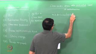
Mod-01 Lec-30 Clean room design and contamination control
Electronic materials, devices, and fabrication by Prof S. Parasuraman,Department of Metallurgy and Material Science,IIT Madras.For more details on NPTEL visit ...
nptelhrd
Metals & Ceramics: Crash Course Engineering #19
Today we'll explore more about two of the three main types of materials that we use as engineers: metals and ceramics. We'll discuss properties of metals, alloys ...
CrashCourse
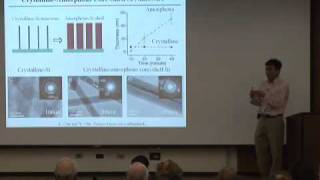
Developing New Semiconductor Materials as Magnets to Realize Semiconductor Spintronics
Keio Spintronics Network - Kuroda Laboratory , University of Tsukuba Graduate School of Pure and Applied Sciences (Materials Science and Engineering)] At ...
慶應義塾Keio University
What is Materials Engineering?
STEMerch Store: https://stemerch.com/Support the Channel: https://www.patreon.com/zachstar PayPal(one time donation): https://www.paypal.me/ZachStarYT ...
Zach Star
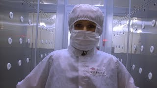
Inside The Worlds Largest Semiconductor Factory - BBC Click
We visit the worlds largest semiconductor factory in Taipei, Taiwan. Subscribe HERE http://bit.ly/1uNQEWR Find us online at www.bbc.com/click Twitter: ...
BBC Click
Lecture 32 (CHE 323) Semiconductor Manufacturing Yield
Semiconductor Manufacturing: Yield and Defects.
Chris Mack
Beyond Moore’s Law: 3D Semiconductor Technologies
What is 3D semiconductor packaging and how will it shape the electronics industry? With decades of experience and proven leadership in semiconductor ...
Xperi Corp
Science Talks Lecture 15: Pervoskite Semiconductors Nanocrystals - Lights, Electrons, Action
ACS Science Talks features a series of lectures by many researchers in different diverse fields of chemistry from around the world. In this video, Angshuman Nag ...
American Chemical Society
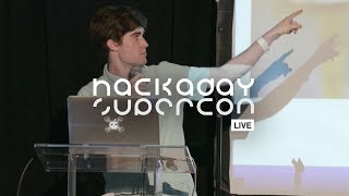
Hackaday Supercon - Sam Zeloof Home Chip Fab: Silicon IC Fabrication in the Garage
IC and semiconductor fabrication techniques, tools, and processes that allow for mid 1970's era device fabrication on a small budget in the home workshop.
HACKADAY
Mod-01 Lec-25 Lithography
Electronic materials, devices, and fabrication by Prof S. Parasuraman,Department of Metallurgy and Material Science,IIT Madras.For more details on NPTEL visit ...
nptelhrd
Lecture 17: Compound Semiconductor Materials Science (Crystal Growth and Phases)
Class information: Taught during Spring 2016 as mse5460/ece5570, at Cornell University by Professor Debdeep Jena. Class website: https://goo.gl/OXsYpY.
Debdeep Jena
What Are Semiconductor Materials?
https://www.fiberoptics4sale.com Semiconductors are made up of individual atoms bonded together in a regular, periodic structure. The electrons surrounding ...
Fiber Optics For Sale Co.
Materials Engineer Salary (2019) – Materials Engineer Jobs
How much does a Materials Engineer make in a year? How many jobs are there for Materials Engineers? How do you become a Materials Engineer? In this ...
CareerWatch
Tutorial: Doping
MIT 2.627 Fundamentals of Photovoltaics, Fall 2011 View the complete course: http://ocw.mit.edu/2-627F11 Instructor: Joe Sullivan Pure silicon has very low ...
MIT OpenCourseWare
Mod-01 Lec-11 Compound Semiconductors
Processing of Semiconducting Materials by Dr. Pallab Banerji,Department of Metallurgy and Material Science,IIT Kharagpur.For more details on NPTEL visit ...
nptelhrd
Department of Materials Science and Engineering, Seoul National University
SNU-MSE, Enabler of Economic Growth of South Korea. South Korea achieved great economic success in many aspects. It is the only country in the world who ...
WebsEdge Science
Los Alamos National Laboratory, Division of Materials Science & Technology
The Science of Materials Certification. In the past, certification of materials in high consequence applications has required decades of work.Today, the Los ...
WebsEdge Science
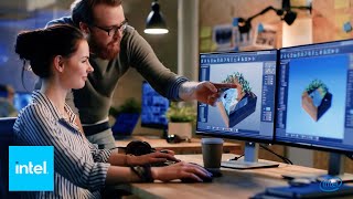
From Sand to Silicon: The Making of a Microchip | Intel
Ever wonder what's under the hood of your favorite electronic device? The transistor is the engine that powers every Intel processor. To build a modern computer ...
Intel
Mod-01 Lec-04 Doping in Semiconductors
Processing of Semiconducting Materials by Dr. Pallab Banerji,Department of Metallurgy and Material Science,IIT Kharagpur.For more details on NPTEL visit ...
nptelhrd
Mod-01 Lec-30 Metal-Semiconductor Contact - II
Processing of Semiconducting Materials by Dr. Pallab Banerji,Department of Metallurgy and Material Science,IIT Kharagpur.For more details on NPTEL visit ...
nptelhrd
Lec-4 | Bulk crystal growth, semiconductor manufacturing, ingots, Wafers | Semiconductors
This lecture deals with the Bulk Crystal growth, starting materials, Ingots and wafers Hi Friends, I welcome you to the world of Electrocombot and Udta engineer.
Udta Engineer
Mod-01 Lec-21 Si wafer manufacturing
Electronic materials, devices, and fabrication by Prof S. Parasuraman,Department of Metallurgy and Material Science,IIT Madras.For more details on NPTEL visit ...
nptelhrd
Paul Nealey - Self-Assembling Materials for Semiconductor Manufacturing
Paul Nealey, Brady W. Dougan Professor, Institute for Molecular Engineering, UChicago; Senior Scientist, Argonne gives a talk about his research at the ...
UChicagoResearch
Introduction to Materials Science for MEMS and NEMS - Part 1
Join Spaceport Odyssey iOS App for Part 2: https://itunes.apple.com/us/app/spaceport-odyssey/id1433648940 Join Spaceport Browser for Part 2: ...
SpaceChallenges
Diffusion: Introduction
Steel for Gear Carburization pn Junction.
Introduction to Materials Science and Engineering
ME260 Ch28 Part IV - Semiconductor Manufacturing
We cover the essential of etch, implant, wire bonding and packaging.
Matthias Pleil
Mod-01 Lec-27 Metallization and polishing
Electronic materials, devices, and fabrication by Prof S. Parasuraman,Department of Metallurgy and Material Science,IIT Madras.For more details on NPTEL visit ...
nptelhrd
Materials Science and Engineering | MISiSx on edX
Discover the various properties and structures of materials and build a solid foundation in engineering. Take this course here: ...
edX
Lisa Porter: Semiconductors for an Energy Efficient Future
Professor of Materials Science and Enginering Lisa Porter discusses her research on semiconductor materials and devices, especially those that enable new ...
College of Engineering, Carnegie Mellon University
Materials Science of Silicon MEMS: A Two-Way Street
EECS 500 Arthur Heuer Friday, September 19th, 2008 MEMS-Micro Electro Mechanical Systems-add sensing and actuation, to the electronic functionality that is ...
Case Western Reserve University
Mod-01 Lec-07 Diffusion and Ion Implantation - I
Processing of Semiconducting Materials by Dr. Pallab Banerji,Department of Metallurgy and Material Science,IIT Kharagpur.For more details on NPTEL visit ...
nptelhrd
Mod-01 Lec-02 Electrical Conductivity of Materials
Processing of Semiconducting Materials by Dr. Pallab Banerji,Department of Metallurgy and Material Science,IIT Kharagpur.For more details on NPTEL visit ...
nptelhrd
Nanomaterials for Batteries & Energy Storage
Yi Cui, associate professor of Materials Science and Engineering at Stanford University, discusses designing nanomaterials for energy storage, including ...
Stanford
? LIGHT EMITTING DIODE or LED - Working Principle explained in HINDI
In this Physics (Digital Electronics) video lecture in Hindi we explained the working principle of light emitting diode, known as LED. Light emmiting diode is made ...
EduPoint
Lec 1 | MIT 2.830J Control of Manufacturing Processes, S08
Lecture 1: Introduction -- processes and variation framework Instructor: Duane Boning, David Hardt View the complete course at: http://ocw.mit.edu/2-830JS08 ...
MIT OpenCourseWare
Semiconductors, and polymers, and metals! Oh my Thin film Materials Processing 20150602 1800 1 1
The second webinar in the 2015 series for FACT Services (Fabrication, Assembly, Characterization, Test) presents service capabilities in materials deposition ...
CMC Microsystems
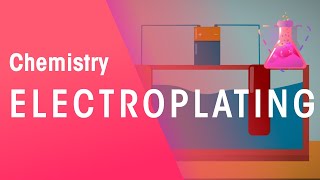
How Does Electroplating Work | Reactions | Chemistry | FuseSchool
How Does Electroplating Work | Reactions | Chemistry | FuseSchool Learn the basics about electroplating. The anode is positively charged, and the cathode is ...
FuseSchool - Global Education
Mod-01 Lec-01 Introduction
Advanced ceramics for strategic applications by Prof. H.S. Maiti,Department of Metallurgy and Material Science,IIT Kharagpur.For more details on NPTEL visit ...
nptelhrd
What’s a compound-semiconductor wafer look like?
David Danzilio of compound semiconductor fab WIN Semiconductor, talks about what goes into such compound semiconductor wafers as comprised of gallium ...
EE World Online
China’s Mega Projects: Manufacturing
Made in China” is a mark that you can see everywhere in the world. Seven out of the world's biggest ports are in China. But the process of manufacturing is ...
CGTN
Mod-03 Lec-21 Carrier recombination-generation-I: band-to-band transition
Optoelectronic Materials and Devices by Prof. Monica Katiyar & Prof. Deepak Gupta,Department of Metallurgy and Material Science,IIT Kanpur.For more details ...
nptelhrd