Semiconductor Fabrication Basics - Thin Film Processes, Doping, Photolithography, etc.
http://wiki.zeloof.xyz http://sam.zeloof.xyz.
Sam Zeloof
12. Thin Films: Material Choices & Manufacturing, Part I
MIT 2.627 Fundamentals of Photovoltaics, Fall 2011 View the complete course: http://ocw.mit.edu/2-627F11 Instructor: Tonio Buonassisi This lecture introduces ...
MIT OpenCourseWare
Thin Film Transistors (TFTS)
Course in Printed Electronics: Thin film transistors (TFTS) by Mid Sweden University. Help us caption & translate this video! http://amara.org/v/5Pr7/
Mittuniversitetet
Printed metal oxide heterojunctions
A vlog of our recent publication in RSC Advances. The video describes our work on the synthesis of a printable nickel oxide ink, and using that to fabricate a ...
Electronic Materials and Thin Films Lab
What is THIN FILM? What does THIN FILM mean? THIN FILM meaning, definition & explanation
http://www.theaudiopedia.com The Audiopedia Android application, INSTALL NOW - https://play.google.com/store/apps/details?id=com.
The Audiopedia
Electroluminescent Devices Based on 2D Semiconducting Transition Metal Dichalcogenides
Excitonic van der Waals semiconductors are an attractive building block for constructing on‐chip nanophotonic devices with unconventional functionalities.
Advanced Science News
nanoHUB-U Thermoelectricity L3.4: Nano/Macroscale Characterization - Thin Film Characterization
Table of Contents: 00:09 Lecture 3.4: Thin Film Thermoelectric Characterization 00:33 Thin film thermal characterization 02:02 Thin film electrical ...
nanohubtechtalks
A Simple Wet Chemical Technique to Prepare Ultrathin Metal Nanwire Thin Films
Lecturer: Gil Markovich, chool of Chemistry, Tel-Aviv University, Tel-Aviv, Israel "The 14th Israel Materials Engineering Conference", Held at the Tel Aviv ...
TAUVOD
5.2 - Thin film silicon PV technology - part I
DelftX: ET3034TUx Solar Energy.
3rab Geeks
Printing the Electronics of the Future | Dr. Troy Townsend | TEDxLeonardtown
Dr. Troy Townsend is a professor and innovator of solar technology. His visionary work in 3D printing has the potential to transform the way we create and ...
TEDx Talks
Pulsed Laser Deposition PLD Explained With Animations
Pulsed laser deposition (PLD) is a technique that allows to prepare thin films of a variety of materials. In this method the target material is irradiated with laser in ...
Captain Corrosion
2D Material Workshop 2018: Devices
2D Materials Devices: Aaron Franklin, Duke University.
Minnesota Nano Center
Electrical Properties of thin film
Subject:Material Science Paper:Thin film science and technology.
Vidya-mitra
ICAM Lecture Series: Electric Field Assisted CVD of Nanostructured Metal Oxide Thin Films
Electric Field assisted Chemical Vapour Deposition of Nanostructured Metal Oxide Thin Films by Dr. Russel Binions. For more BP-ICAM webinars: ...
The BP International Centre for Advanced Materials
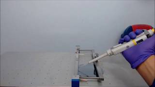
Clear flexible printed circuits - first success
I'm making flexible printed circuits with my vacuum deposition machine. In this video, I show my first successful active circuit built with copper deposited onto ...
Applied Science
Mod-02 Lec-08 Thin-film Materials and their Deposition
Micro and Smart Systems by Prof. K.N. Bhat,Prof. G.K. Anathasuresh,Prof. S. Gopalakrishnan,Dr. K.J. Vinoy, Department of Mechanical Engineering, IISc ...
nptelhrd
Mod-01 Lec-24 Thin Film Deposition
Fabrication of Silicon VLSI Circuits using the MOS technology by Prof. A.N. Chandorkar, Department of Electrical Engineering, IIT Bombay. For more details on ...
nptelhrd
Patterning aluminum with the photoresist "lift-off" method
I show how the photoresist "lift-off" method works to pattern thin films as they are deposited. In this case, I patterned aluminum on a microscope slide.
Applied Science
Superconducting thin films
Subject:Material Science Paper:Thin film science and technology.
Vidya-mitra
Thin-film Photovoltaic (PV) Laminates
Video is from Google video. Installing clean, reliable, inflation-proof solar power is easier than ever, thanks to the invention of thin-film photovoltaic (PV) ...
David Brown
PARC Cleanroom Services: Thin-Film Electronics & Optoelectronic Devices
At PARC, we've leveraged our deep expertise in large-area thin-film electronics and optoelectronic devices to help clients develop novel prototypes and ...
PARC, a Xerox Company
Thin Film Electronics connects the Physical and Digital Worlds
Davor Sutija describes how Thin Film Electronics ASA is enabling near-field communications technologies to connect people and objects, moving from an ...
NanotechnologyVideo
"SOLAR METAL ROOFING: Thin Film PV Panels Installation" by CoolFlatRoof.com
Unisolar PV Panels (136 W)" - $216 each - http://amzn.to/29GZ5mt SOLAR METAL ROOFING: Thin Film PV Panels Installation" by CoolFlatRoof.com ▻ More ...
coolflatroof
Semiconductor based optical sensor
Subject: Material Science Paper: Semiconductor material and devices.
Vidya-mitra
The Science and Technology of Thin Films and Coatings
This is a seminar that presents a brief introduction into thin films and coatings science and technology, including materials science, deposition and synthesis ...
Mohammad Al-Kuhaili
Mod-04 Lec-40 Organic Solar Cells and Organics Thin Film Transistors
Optoelectronic Materials and Devices by Prof. Monica Katiyar & Prof. Deepak Gupta,Department of Metallurgy and Material Science,IIT Kanpur.For more details ...
nptelhrd
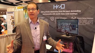
Waterproofing electronics: HZO Protects What Matters Most To You using thin-film nanotechnology
According to IDC, by 2025, there will 41.6 billion connected IoT devices. Devices we rely on for a variety of important tasks. It's critical that these devices function ...
Charbax
Discovery of new transparent thin film material could improve electronics and solar cells
A team of researchers, led by the University of Minnesota, have discovered a new nano-scale thin film material with the highest-ever conductivity in its class.
TECH-TUBE
Surface Chemistry - Thin Film Experiments with Dr Irving Langmuir
This film comes from the 'Nobel Science Series' from the American Institute of Motion Pictures. Filmed in 1939, it shows Doctor Irving Langmuir, who won the ...
Ri Archives
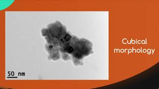
Nano-metal based sensors
By: Zyad Shehata Day B.
AUSC UST
Thin-Film Silicon PV Technology
Learn about a different silicon technology, the thin-film silicon PV technology, which belongs to the so-called second generation PV technology. Take the full ...
edX
The World Of Microscopic Machines
Micro-electromechanical systems or MEMS are tiny integrated devices that combine mechanical and electrical components. Traditional manufacturing ...
New Mind
5.2 - Thin film silicon PV Technology - part II
DelftX: ET3034TUx Solar Energy.
3rab Geeks
Epitaxial Lift-Off of Centimeter-Scaled Spinel Ferrite Oxide Thin Films for Flexible Electronics
Flexible centimeter-scaled single-crystalline spinel ferrite oxide thin films are transferred onto plastic substrates using a simple method. The transferred thin films ...
Advanced Science News
INTRODUCTION TO THIN FILMS - what is a thin film?
INTRODUCTION TO THIN FILMS - what is a thin film? : If the incident light is broadband, or white, such as light from the sun, interference patterns appear as ...
e Tution
Mod-01 Lec-11 Pulsed Laser Deposition: Oxide thin films
Chemistry of Materials by Prof.S.Sundar Manoharan,Department of Chemistry and Biochemistry,IIT Kanpur.For more details on NPTEL visit http://nptel.ac.in.
nptelhrd
No. 12. Applications II: Properties of thin films, stress/strain, deformation potentials
Applications II: Properties of thin films, stress/strain, deformation potentials.
Akademie věd České republiky
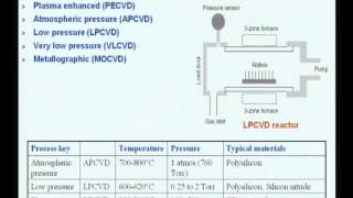
Chemical Vapour Deposition (CVD)
Chemical Vapour Deposition (CVD)
Surface Engineering of Nanomaterials
Liquid metal | Michael Dickey | TEDxNCSSM
Dr. Dickey received a BS in Chemical Engineering from the Georgia Institute of Technology and a PhD in Chemical Engineering from the University of Texas at ...
TEDx Talks
Thin Film Deposition through Gas Phase Techniques
Thin Film Deposition through Gas Phase Techniques.
Surface Engineering of Nanomaterials
Electronic Structure of Graphite Thin Films
2010/6/2 Osaka,G-COE Electronic Structure of Graphite Thin Films , S.Okada , University of Tsukuba.
慶應義塾Keio University
Expeditious, scalable solution growth of metal oxide films by combustion blade coating for flexible
Expeditious, scalable solution growth of metal oxide films by combustion blade coating for flexible electronics. Binghao Wang et al (2019), PNAS ...
ScienceVio